
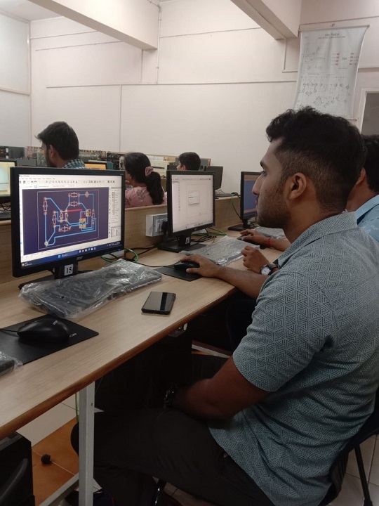
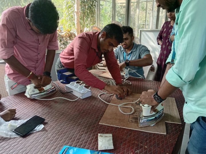
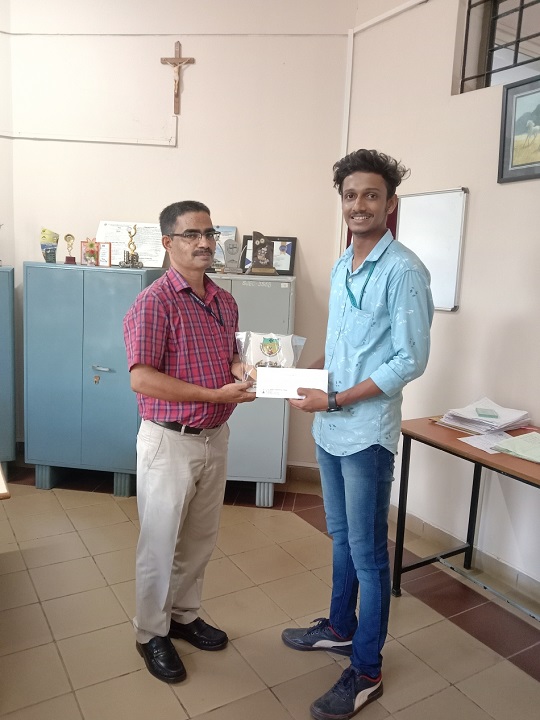
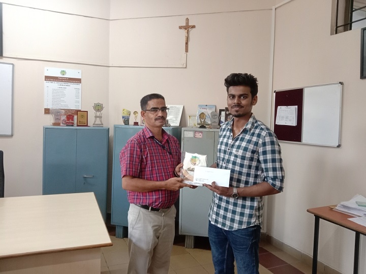
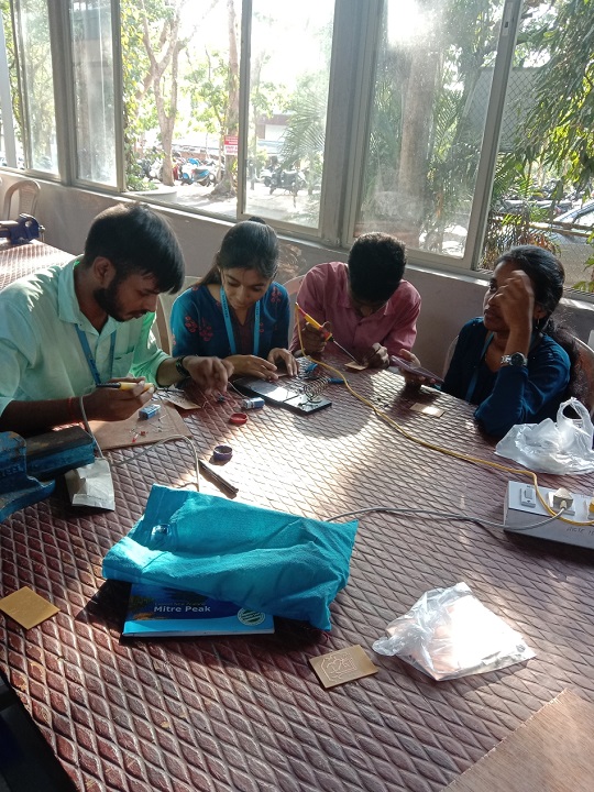
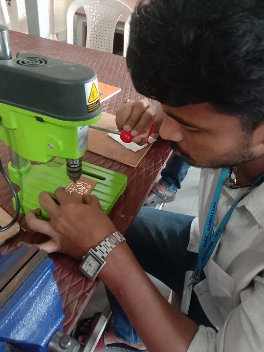
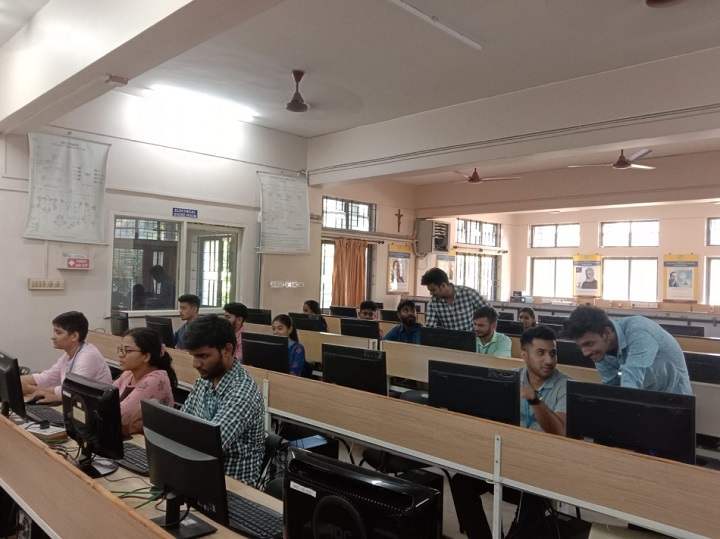
One day hands on training session on "PCB Design and Fabrication using KiCad Software” was organized by the Department of Electrical and Electronics Engineering & Department of Civil Engineering in association with SJEC AICTE Idea Lab & IEEE SJEC student Chapter- PES for the III year students of EEE and Civil Engineering Department on 5 June 8, 2023. The final year studentsMr Rajath Kumar & Mr ManojKulal from the dept. of EEE were the resource persons. The motive of training was to enhance knowledge of students on PCB design skills. A brief introduction was given on a schematic capture tool to create PCB layout, understanding the electrical parameters and creating the schematic. The resource team also explained to define design rules and requirements,placing of the components, route the traces and generating design/layout files. Participants were given hands on exercise to create the schematic of op-amp tester circuit, PCB etching, drilling and soldering. The outcome of the training has enabled the students to gain an in-depth practical knowledge on using KiCad software for building mini projects andmain project. The training session provided a great opportunity for interested students inelectronic projects to lea new skills. The program was coordinated by Ms MadhaviGatty and Mr Rohith Veigas - Assistant Professors from Dept. of EEE and Civil Engineering.

Leading engineering college in Mangalore offering BE, MBA & MCA programs with strong placements, modern campus, hostels and student support.
© SJEC is Made with by Siona Solutions