
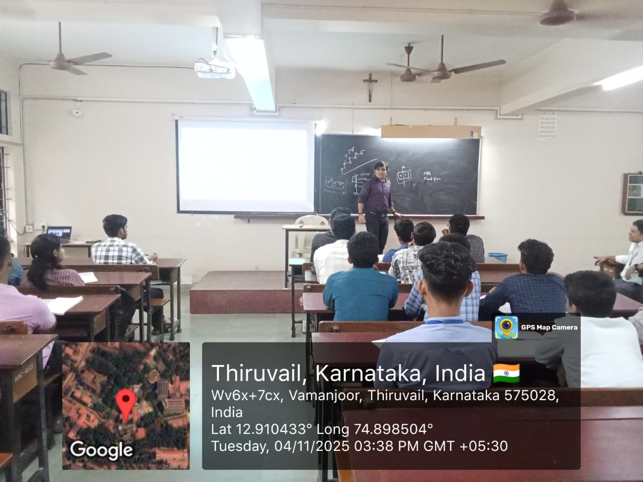
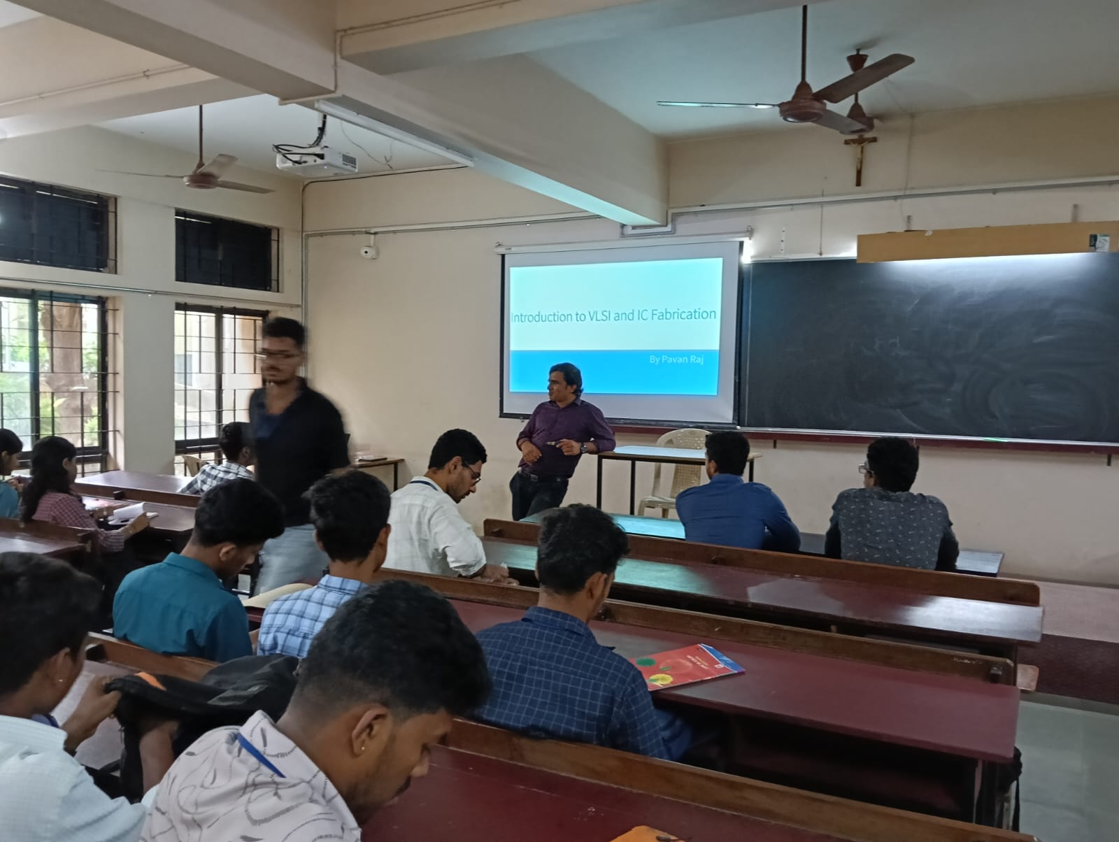
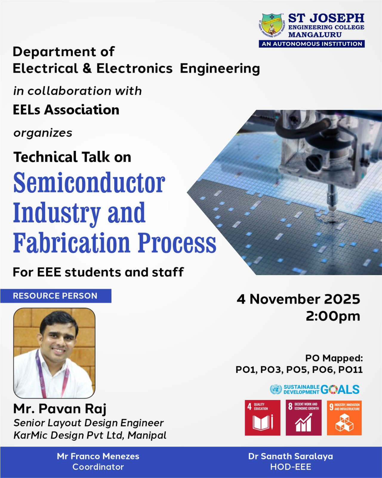
The Department of Electrical and Electronics Engineering, in association with the EELs Association, organized a technical talk on “Semiconductor Industry and Fabrication Process” for the final-year EEE students on 04 November 2025. Mr Pavan Raj, Senior Layout Design Engineer, KarMic Design Pvt Ltd,Manipal was the resource person.
The session aimed to provide students with an in-depth understanding of the semiconductor industry, its fabrication processes, and the emerging opportunities in the VLSI sector. The resource person elaborated on the various stages involved in semiconductor device manufacturing; the cleanroom environment, wafer processing, and testing methodologies used in modern fabrication plants.
In addition to the technical aspects, the talk also focused on career readiness and interview preparation for students aspiring to enter VLSI and semiconductor industries. The session emphasized the key skills, tools, and concepts expected from graduates during placement interviews in core companies.
The talk was highly interactive and enriched the participants’ awareness of current industry practices, challenges, and technological trends shaping the semiconductor domain. The event concluded with a Q&A session, where students actively clarified their doubts and gained valuable insights for their professional development.
The department expressed gratitude to the EELs Association for organizing the event and to the resource person for delivering an informative and inspiring session.

Leading engineering college in Mangalore offering BE, MBA & MCA programs with strong placements, modern campus, hostels and student support.
© SJEC is Made with by Siona Solutions