
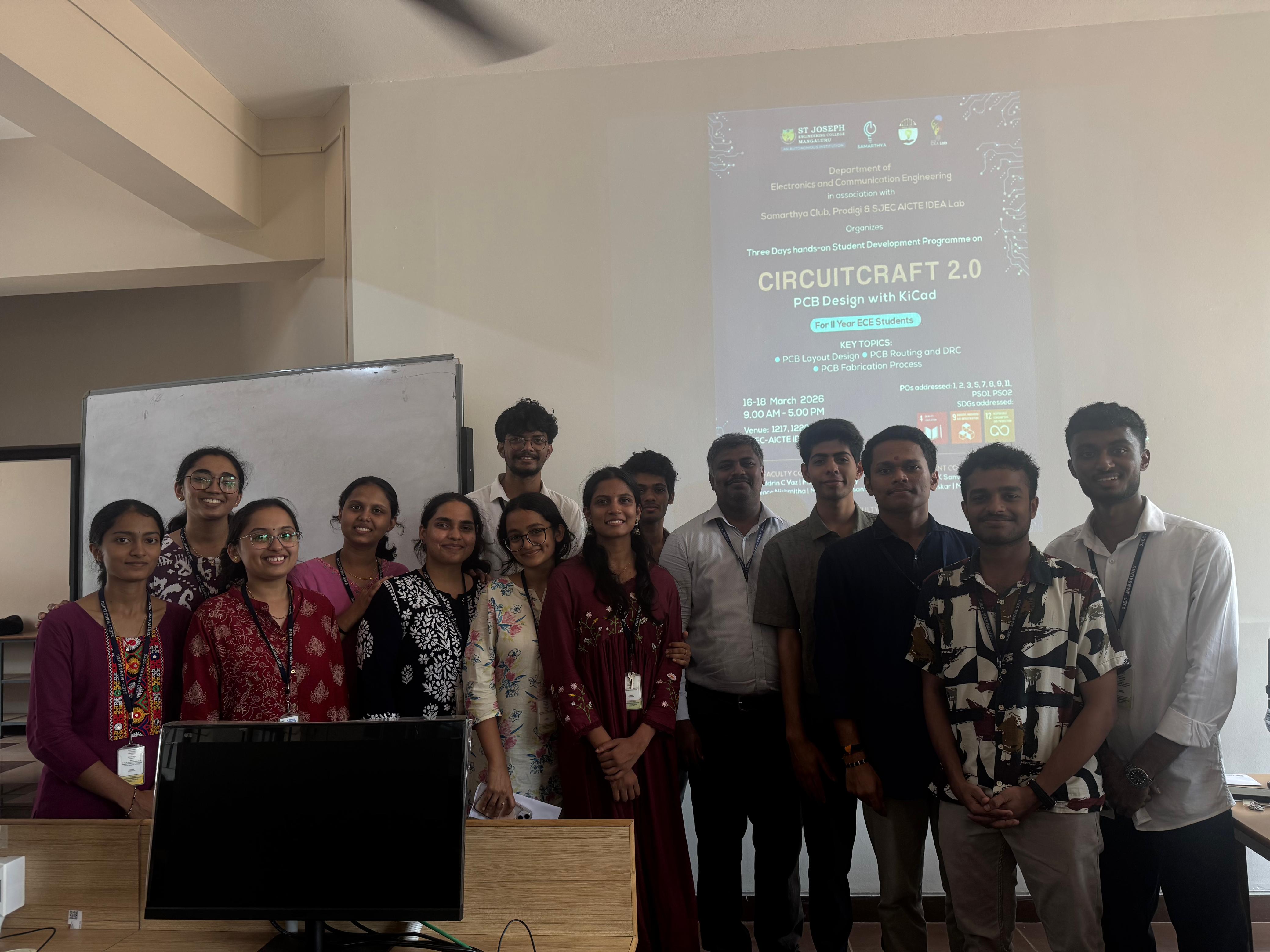
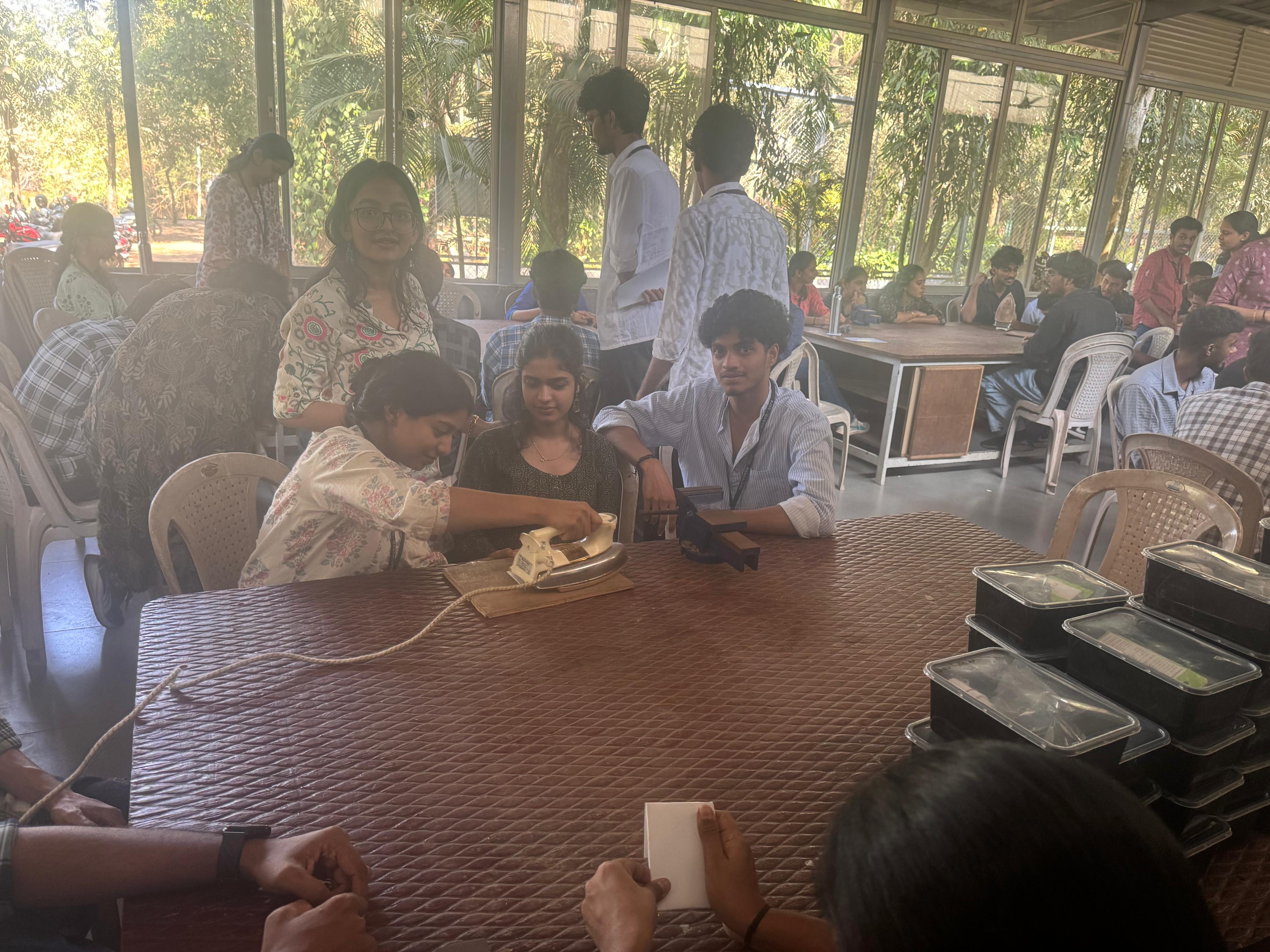
The Department of Electronics and Communication Engineering, in association with the Samarthya Club, Prodigi Association, and the SJEC AICTE IDEA Lab, successfully conducted a three-day hands-on Student Development Program (SDP) titled “CircuitCraft: PCB Design Using KiCad” from 04 to 06 February 2026 for 6th semester ECE students, followed by “CircuitCraft 2.0: PCB Design Using KiCad” from 16 to 18 March 2026 for 4th semester ECE students.
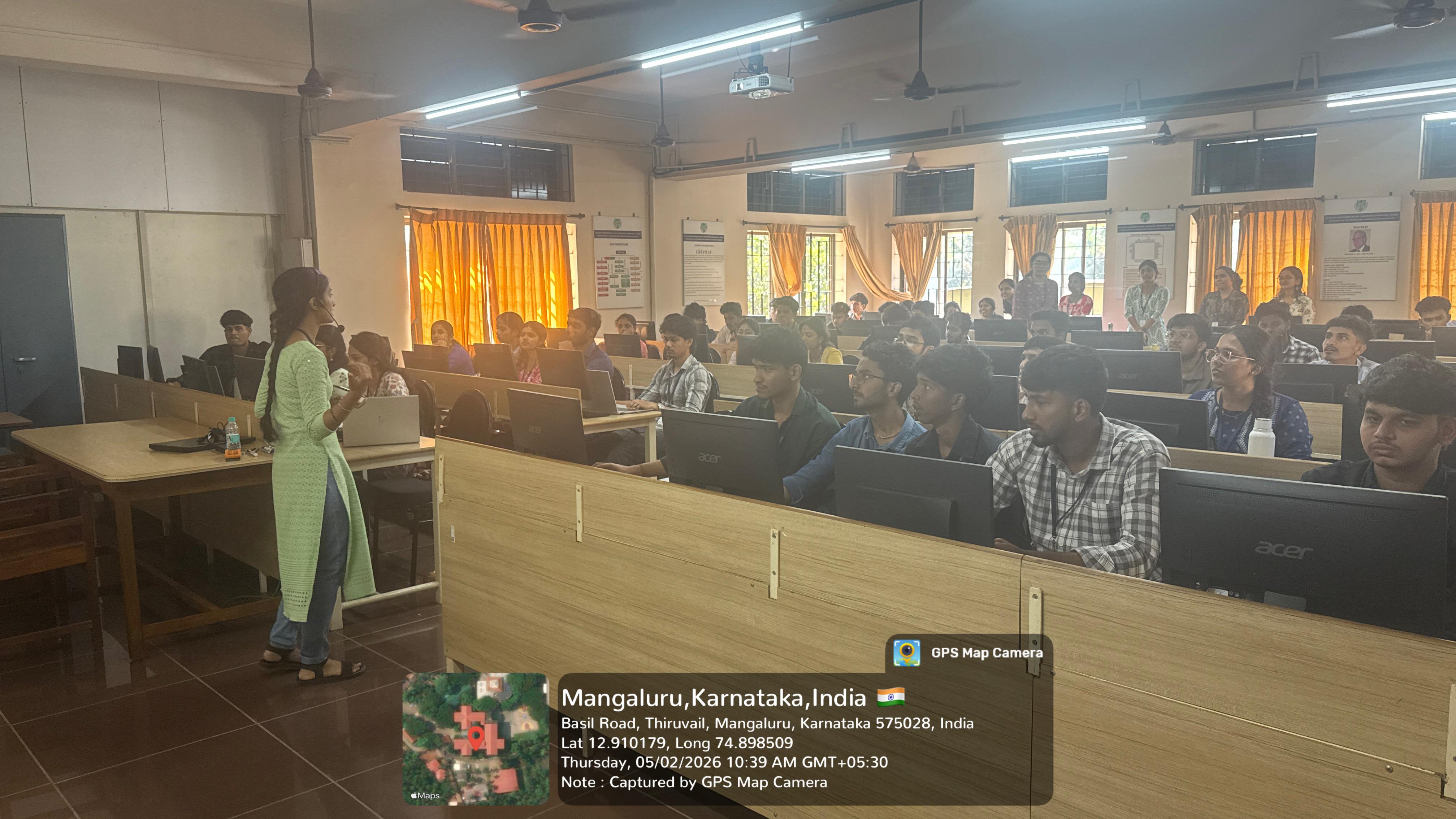
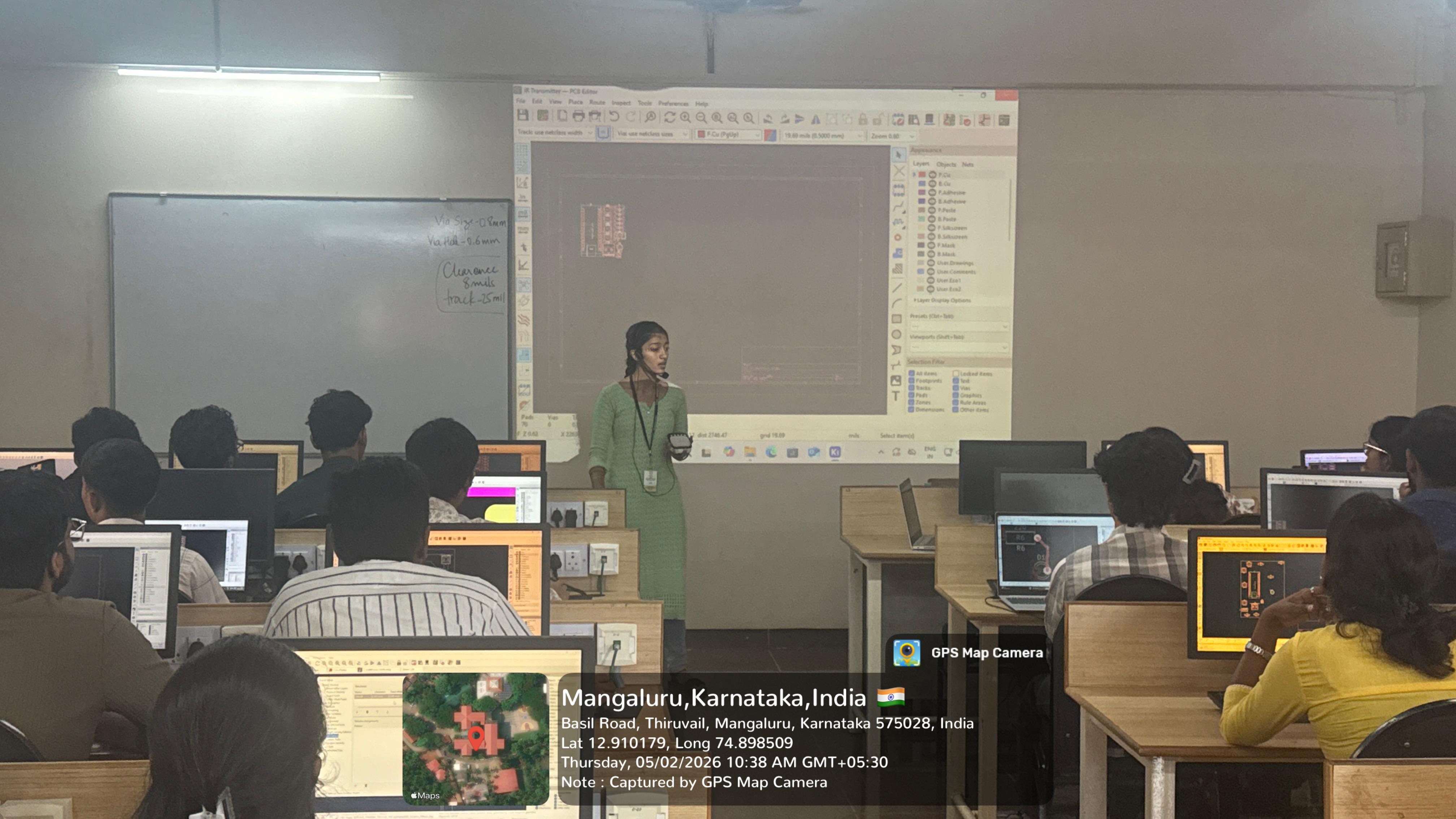
The SDP offered comprehensive training on the complete PCB design workflow, including schematic capture, component selection, footprint assignment, PCB layout design, routing, design rule checks, and fabrication file generation. Participants were introduced to industry-standard design practices and gained practical exposure to the KiCad software platform.
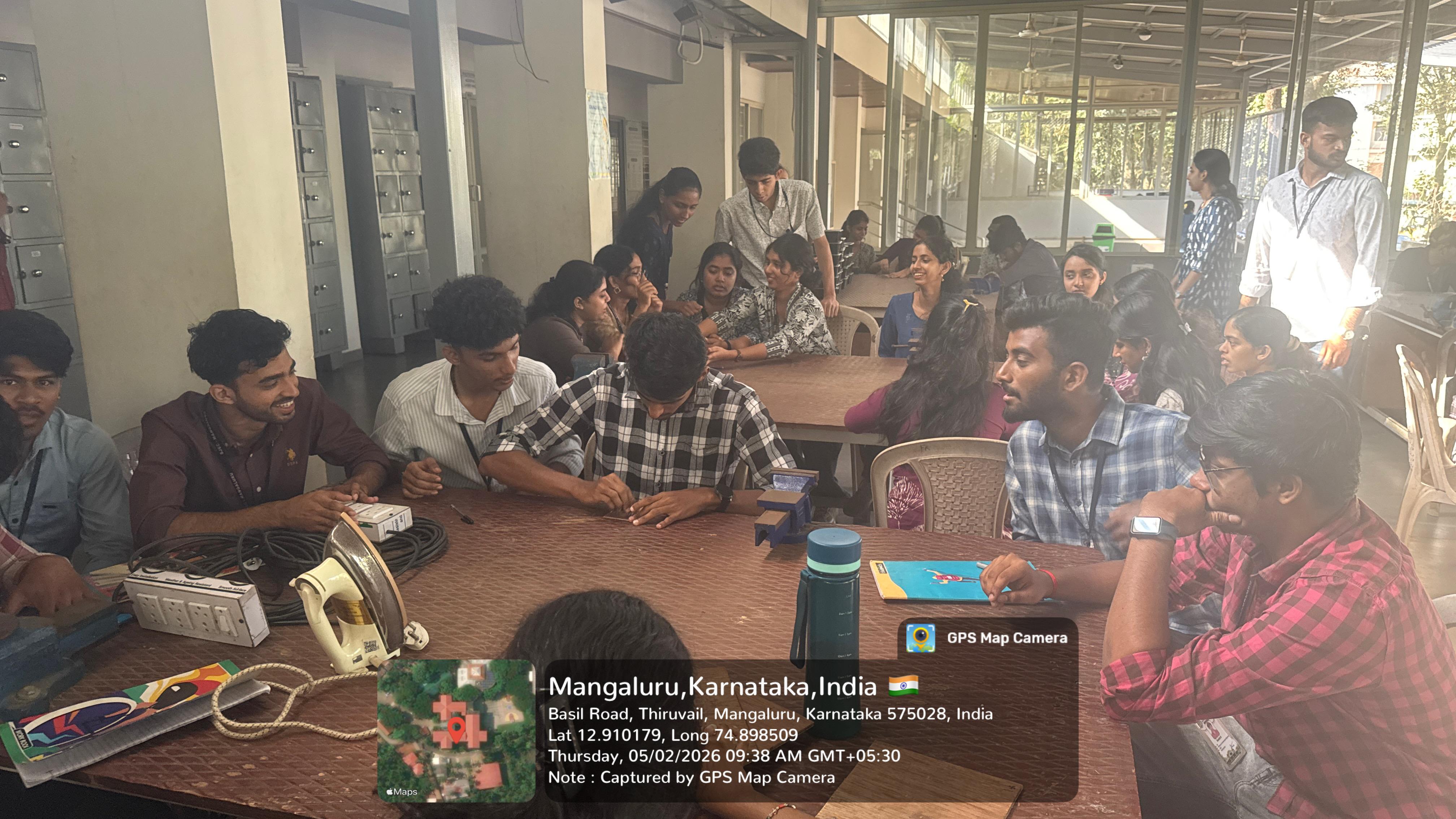
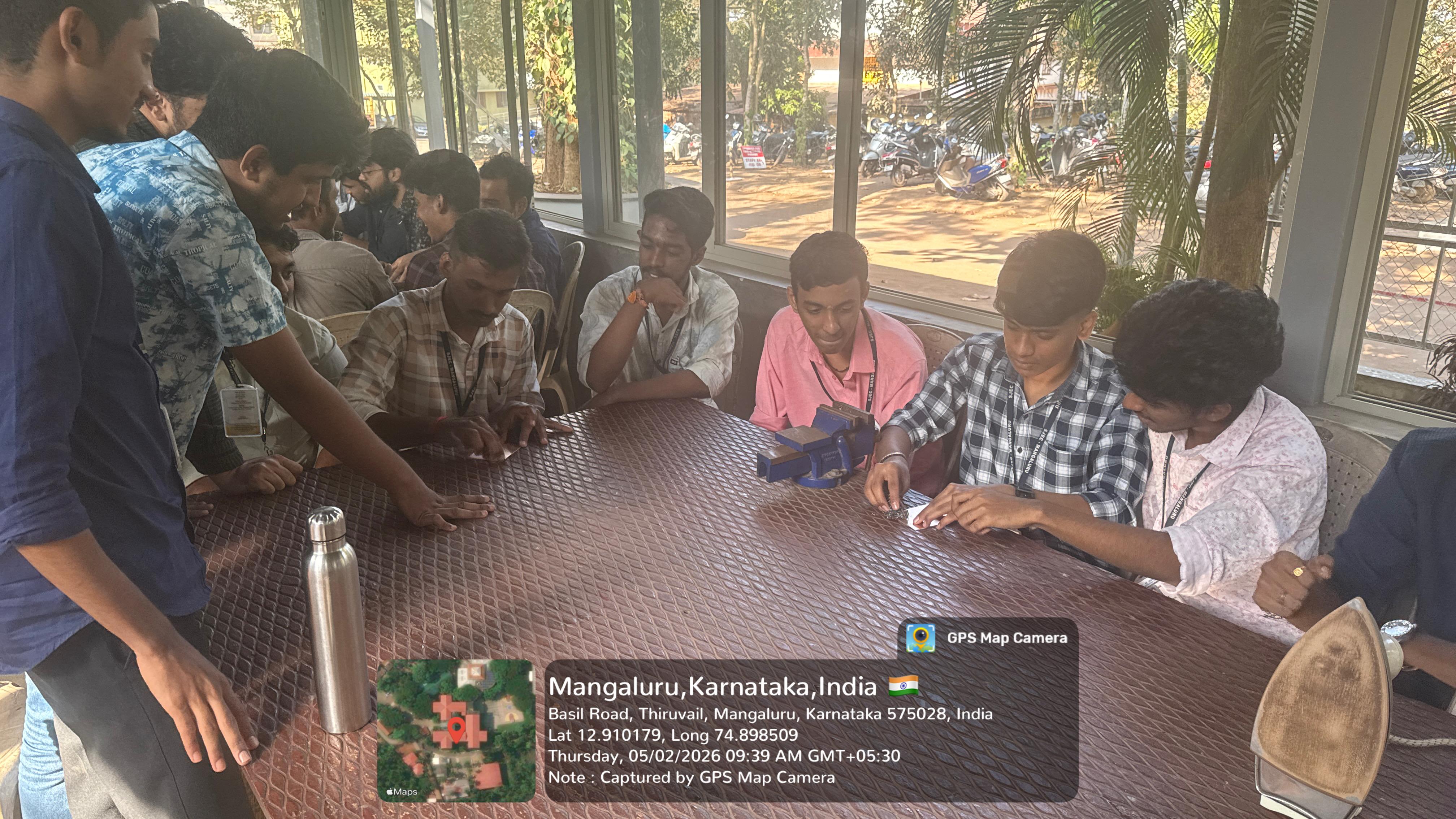
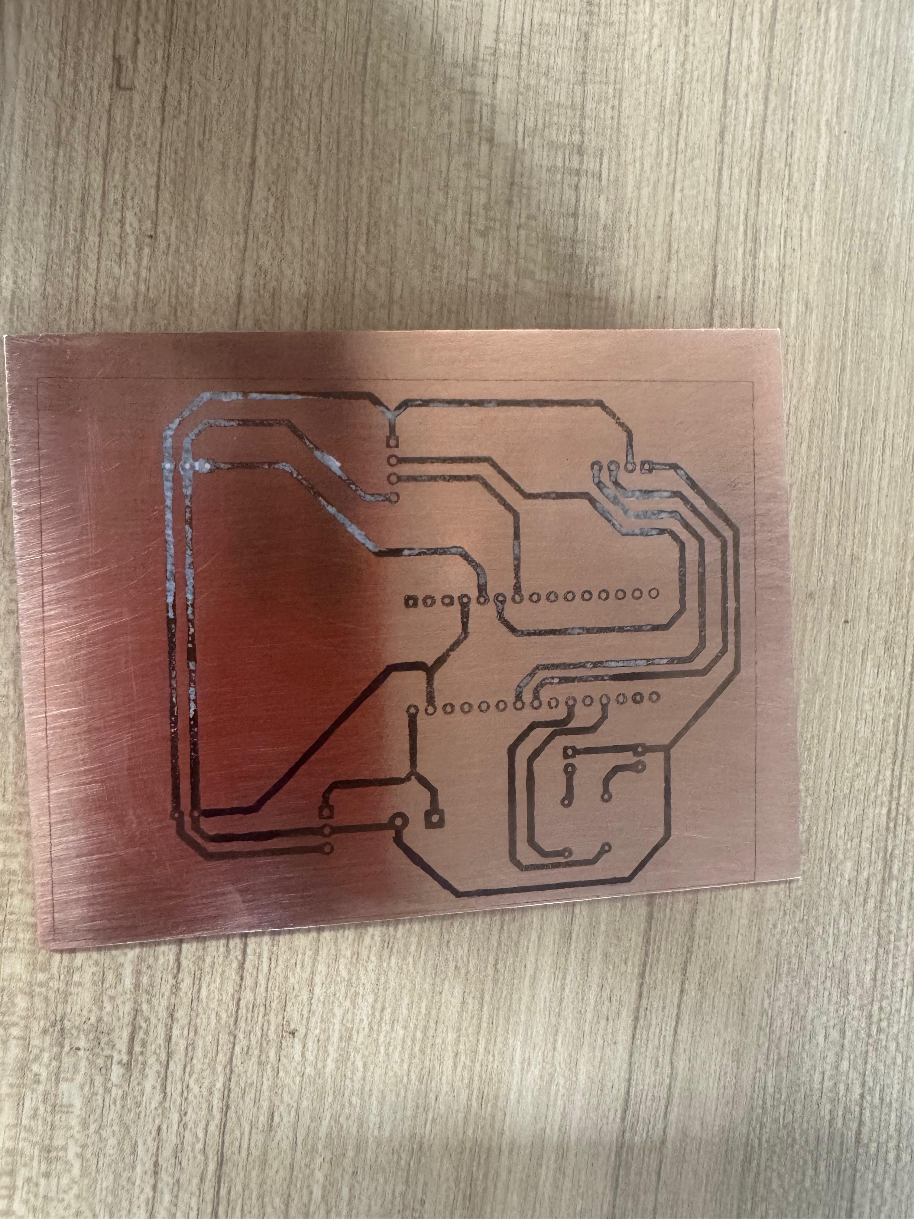
As part of the hands-on sessions, students designed and developed an Infrared (IR) receiver circuit, converting their schematics into functional PCB layouts. The training emphasized real-time troubleshooting, design optimization, and adherence to best practices in PCB design. Overall, the program significantly enhanced students’ practical skills and confidence in independently executing hardware projects, effectively bridging the gap between theoretical knowledge and real-world application.

Leading engineering college in Mangalore offering BE, MBA & MCA programs with strong placements, modern campus, hostels and student support.
© SJEC is Made with by Siona Solutions